About Us
For years, we have served as the driving force behind the R&D efforts of China’s top research institutions and leading enterprises. Today, Nexalyt Lab brings this proven expertise to the global stage. Equipped with advanced instrumentation, a PhD-led technical team, and an agile service model, we tackle complex challenges in the fields of materials science and semiconductors.
Our core advantage lies in bridging the gap between "lab innovation" and "industrial application". Whether it is analytical testing for advanced semiconductor processes, analytical testing for new materials, or micro-nano processing, we can transform your technical needs into implementable outcomes in an efficient, accurate, and cost-effective manner.
Our Service
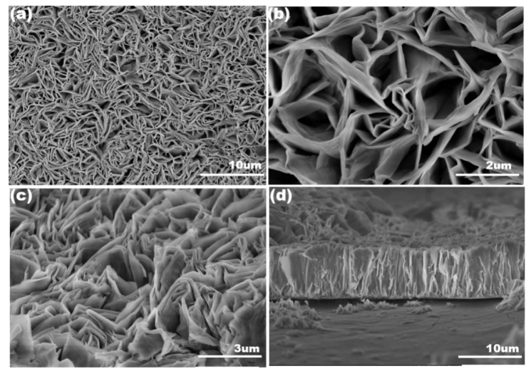
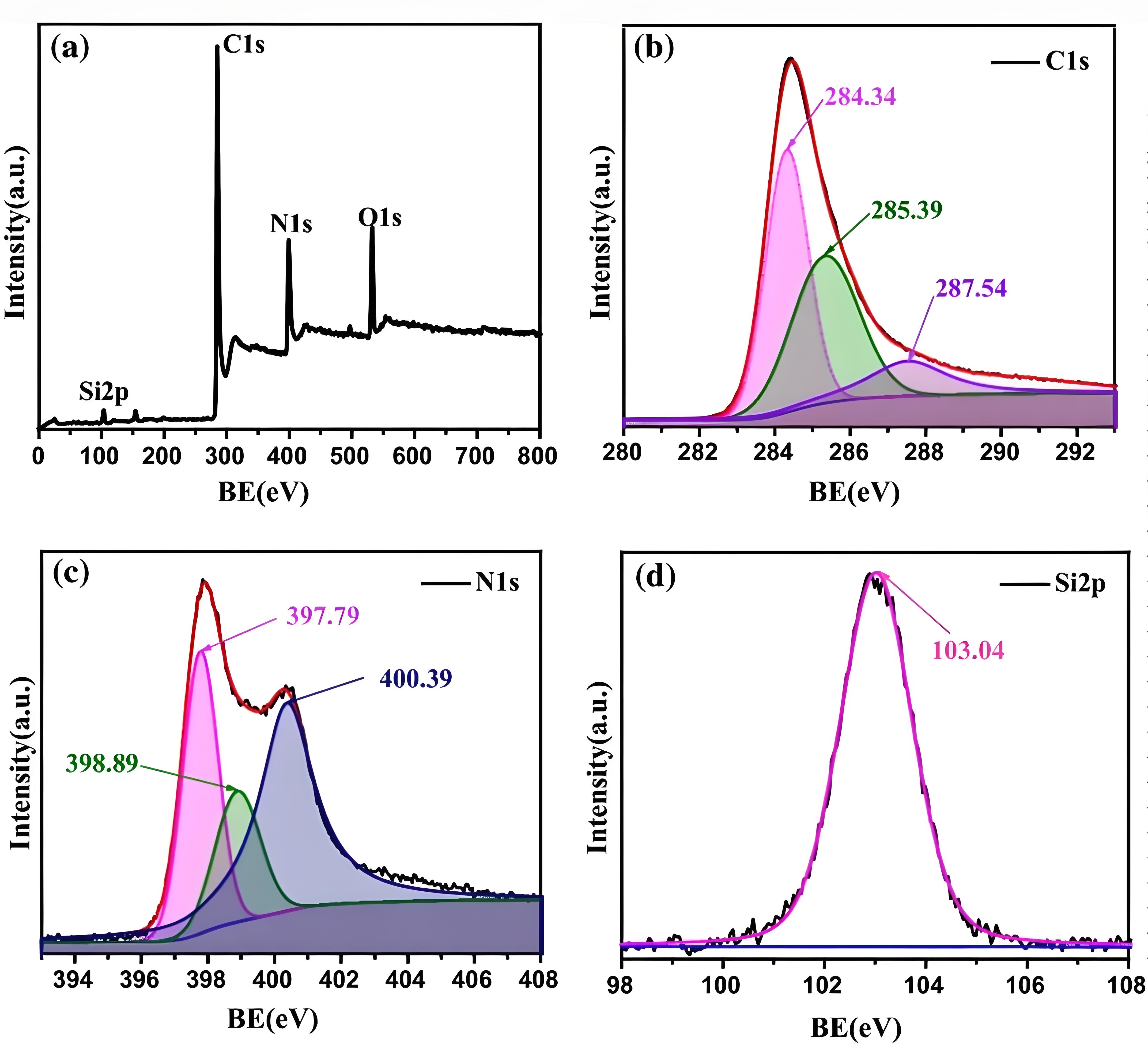
Transmission Electron Microscope (TEM/STEM), Aberration-Corrected Transmission Electron Microscope(ACTEM), Scanning Electron Microscope (SEM)Electronic report delivery within 48 hours
Nuclear Magnetic Resonance (NMR), Magnetic Property Testing, Vickers/Rockwell Hardness Testing, Second Harmonic Generation (SHG) Detection 3 to 7 business days
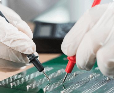
IGBT Device Testing and Evaluation, 8-Inch Wafer Coating, Photomask Design and Fabrication, and Ion Beam Etching (IBE) 3 to 7 business days
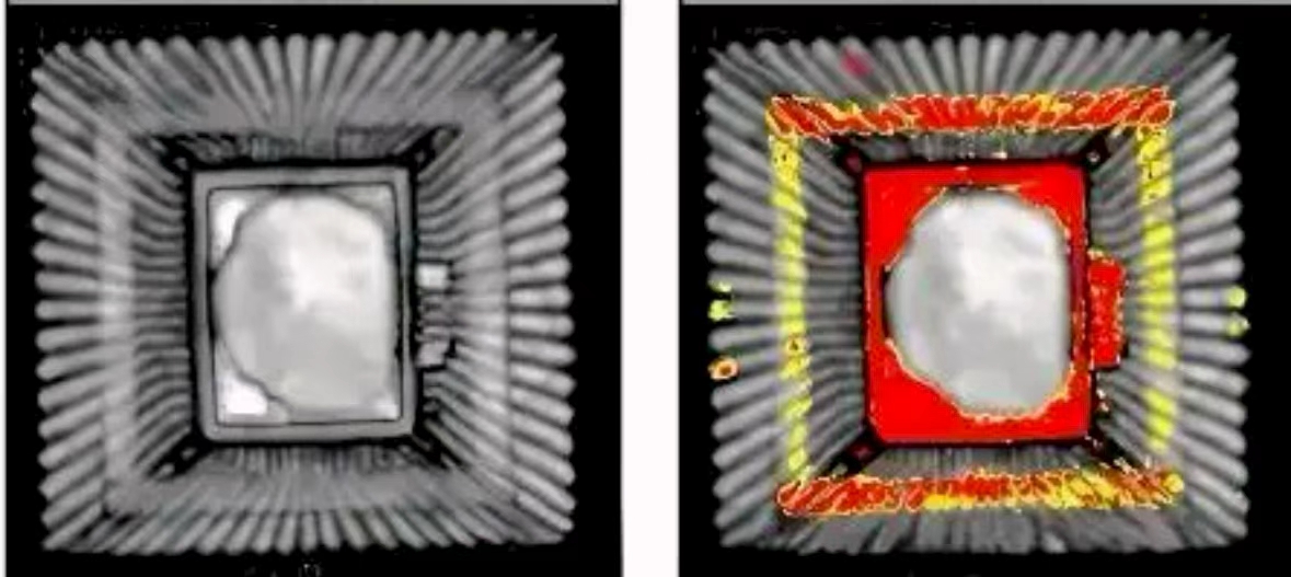
Preparation of STO Wafers with Atomic-Level Flatness, Micro-CT Structural Analysis, Failure Analysis for LED Chips and Other Devices 5 to 7 business days
Project Scheme Customization, Technical Troubleshooting, Joint R&D Cooperation 24-Hour Response
Our Advantages: Reasons to Choose Nexalyt Lab

Over 200 core technical personnel (engineers, technical managers) and more than 1,000 cooperative engineers worldwide, covering fields such as microelectronics, materials science, and physics;
Over 20,000 sets of shared and in-house advanced instruments (e.g., FIB, SEM, TEM, STEM), meeting testing needs in all scenarios;
24-hour response and efficient delivery (for electron microscopy services), with a dedicated contact person to sync progress in real time, keeping you informed of project dynamics at all times;
Having served over 2,000 enterprises and top institutions (e.g., Peking University, Chinese Academy of Sciences, leading IGBT/LED manufacturers) and successfully completed more than 10,000 projects.
Win-Win Cooperation: start Your R&D Project Now

Submit Requirements: Inform your testing, analysis or customization requirements through the online form. Get a Free Proposal: Our team will respond within 24 hours, providing a customized plan, transparent quotation, and timeline;Track & Deliver: Real-time checking of project progress, and after delivery, synchronous verification of data, reports and subsequent technical support.

Institutional Onboarding: Join our network of over 500 cooperative laboratories to share equipment resources, undertake global projects, and expand service scope;Expert Certification: Become a Nexalyt-certified technical expert to participate in high-value R&D projects and access exclusive resources;Strategic Cooperation: Jointly establishing laboratories, developing industry-specific solutions, and conducting media/academic collaborations, we offer technical and operational support.